Anton Simeonov Ph.D. National Institute of Health
Analysis of Life Technologies’ Ion Torrent sequencing platform points to significance of photon-free technology.
ASSAY & Drug Development Technologies offers a unique combination of original research and reports on the techniques and tools being used in cutting-edge drug development. The journal includes a “Literature Search and Review” column that identifies published papers of note and discusses their importance. GEN presents one article that was analyzed in the “Literature Search and Review” column, a paper published in Nature 2011 (475:348–352) titled “An integrated semiconductor device enabling non-optical genome sequencing.” Authors of the Nature paper are J.M. Rothberg, W. Hinz, T.M. Rearick, J. Schultz, W. Mileski, M. Davey, J.H. Leamon, K. Johnson, M.J. Milgrew, M. Edwards, et al.
Abstract from Nature
The seminal importance of DNA sequencing to the life sciences, biotechnology and medicine has driven the search for more scalable and lower-cost solutions. Here we describe a DNA sequencing technology in which scalable, low-cost semiconductor manufacturing techniques are used to make an integrated circuit able to directly perform non-optical DNA sequencing of genomes. Sequence data are obtained by directly sensing the ions produced by template-directed DNA polymerase synthesis using all-natural nucleotides on this massively parallel semiconductor-sensing device or ion chip. The ion chip contains ion-sensitive, field-effect transistor-based sensors in perfect register with 1.2 million wells, which provide confinement and allow parallel, simultaneous detection of independent sequencing reactions. Use of the most widely used technology for constructing integrated circuits, the complementary metal-oxide semiconductor (CMOS) process, allows for low-cost, large-scale production and scaling of the device to higher densities and larger array sizes. We show the performance of the system by sequencing three bacterial genomes, its robustness and scalability by producing ion chips with up to 10 times as many sensors and sequencing a human genome.
Commentary
The field of whole-genome sequencing has been experiencing phenomenal growth and transformation. Benchtop instruments capable of sequencing entire genomes within a fraction of the time the process took a year or two ago have become reality. Most of the so-called Next-Gen sequencing instruments are still based on different versions of fluorescence detection, which in turn requires the use of specialized fluorescent reagents in combination with complex optical systems, both of which contribute to keeping the platforms relatively expensive. The instrument and detection system described by Rothberg and colleagues is unique in its avoidance of light-based detection. Instead, the team from Ion Torrent, presently Life Technologies, makes use of a complementary metal-oxide type of semiconductor sensing device. The basic premise of the technology is that upon polymerase-catalyzed primer extension, a proton is liberated as a result of the deoxynucleotide triphosphate hydrolysis; in turn, the localized change in pH triggered by the liberated proton is detected as a voltage change by the semiconductor sensor (Figure 1).
Figure 1 [Taken from Nature article]: Sensor, well and chip architecture. (a) A simplified drawing of a well, a bead containing DNA template, and the underlying sensor and electronics. Protons (H+) are released when nucleotides (dNTP) are incorporated on the growing DNA strands, changing the pH of the well (ΔpH). This induces a change in surface potential of the metal-oxide-sensing layer, and a change in potential (ΔV) of the source terminal of the underlying field-effect transistor.
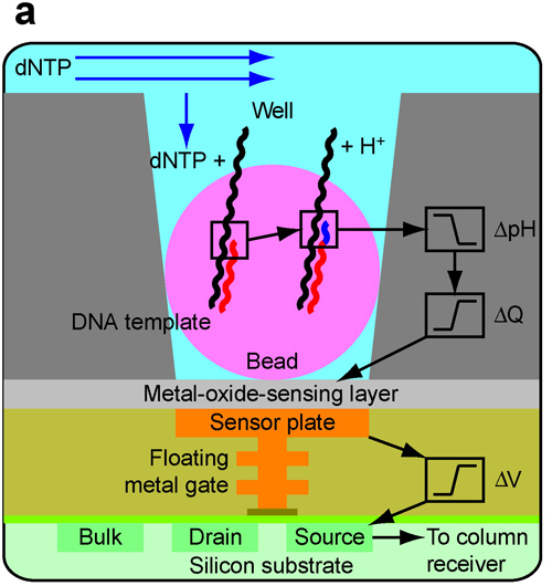
Figure 1 (a)
(b) Electron micrograph showing alignment of the wells over the ISFET metal sensor plate and the underlying electronic layers.
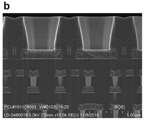
Figure 1 (b)
(c) Sensors are arranged in a two-dimensional array. A row select register enables one row of sensors at a time, causing each sensor to drive its source voltage onto a column. A column select register selects one of the columns for output to external electronics.
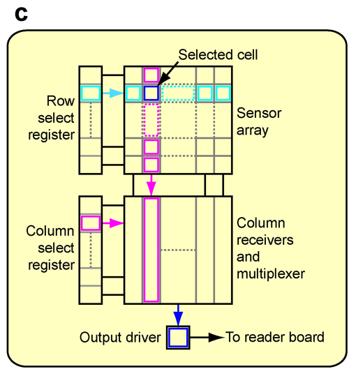
Figure 1 (c)
The team leverages the capabilities of today’s semiconductor manufacturing to deliver very cheap, yet highly reliable, complementary metal-oxide semiconductor (CMOS) integrated circuits in a wide range of sizes and features. To enable high-throughput sequencing, a multi-well chip was developed that incorporated the CMOS on the bottom, while a 3-μm-thick patterned dielectric layer on top was used to form an array of microscopic wells. The entire chip was incorporated within a polycarbonate flow cell, thus allowing facile sample loading and washing (Figure 2).
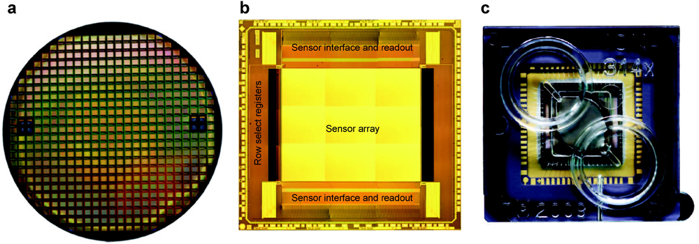
Figure 2: Wafer, die and chip packaging. (a) Fabricated CMOS 8” wafer containing approximately 200 individual functional ion sensor die. (b) Unpackaged die, after automated dicing of wafer, with functional regions indicated. (c) Die in ceramic package wire bonded for electrical connection, shown with moulded fluidic lid to allow addition of sequencing reagents. [Taken from Nature article]
The genomic DNA was fragmented to prepare for sequencing and used to make adaptor-ligated library, which was clonally amplified onto beads. The beads carrying template strands were mixed with sequencing primers and polymerase and loaded onto the chip. The size of the bead particle was chosen to enable a sufficient number of template copies to be loaded into each well in order to ensure adequate signal. During the sequencing run, the four nucleotides were fed in a sequential manner, with brief washes in between. Upon incorporation of one or more of the correct bases, one or more protons were liberated and the magnitude of the voltage output of the CMOS detector was proportional to the number of incorporated bases; the voltage changes produced by each well were then used to perform base calling (Figure 3).
In multiple validation experiments performed on both prokaryotic and eukaryotic genomes, the authors noted a high degree of accuracy and routine acquisition lengths of at least 100 bases. In addition, the team sequenced the whole genome of one male donor and compared the sequence obtained with the present technology to that derived from the ABI SOLiD platform: the sequences were cross-validated at greater than 99.9%. The new “photon-free” technology is expected to be a welcome addition to the arsenal of sequencing groups and other organizations. Further improvements to the system, as noted by the authors, include optimization of the template preparation and signal processing protocols, with the aim to increase the yield of usable reads from the sensors within the chip.

Figure 3: Data collection and base calling. (a) A 50×50 region of the ion chip. The brightness represents the intensity of the incorporation reaction in individual sensor wells. (b) 1-nucleotide incorporation signal from an individual sensor well; the arrow indicates start of incorporation event, with the physical model (red line) and background corrected data (blue line) shown. (c) The first 100 flows from one well. Each colored bar indicates the corresponding number of bases incorporated during that nucleotide flow. [Taken from Nature article]
With the breadth of advances including the Ion Torrent platform in next-gen sequencing, challenges have shifted from finding the right instrument to sample prep and data analysis. For more on these issues, click here to read an article from GEN’s Mar. 1 issue.
Anton Simeoniv works at the NIH.

