Source: luchschen/Getty Images
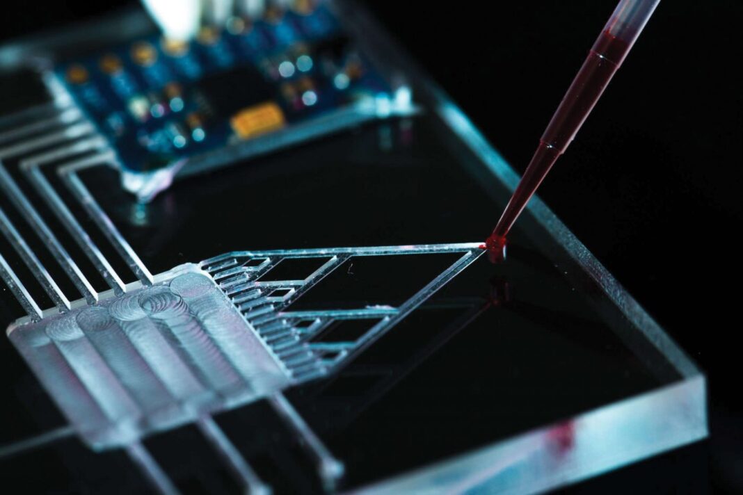
Microfluidic devices, also known as lab-on-a chip devices, tend to be disposable cartridges that contain some or all the chemistry needed for the performance of an assay. Some microfluidic devices require no additional instrumentation. One such device is the common lateral flow assay (LFA) device, which may display a color change after sample is added. Other microfluidic devices do require additional instrumentation. For example, they may require delivery of a cartridge to an optical or fluorescence scanning instrument for results to be read. In all cases, the small size of the cartridge and small volume of reagent requires dependable error-resistant manufacturing processes to ensure product quality.
The movement toward microfluidics in lab-on-a-chip design mimics the technology conversions seen in other aspects of the medical diagnostic industry in past generations, such as the use of textile dyes for cellular and molecular staining. In microfluidics, several technologies developed for use in other industries are being adapted. These technologies include digital liquid dispensing (from the printing industry), injection molding (from compact disc manufacturing), and photolithography (from the semiconductor industry).
In the microfluidics industry, diverse technologies, including ones matured in other industries, are helping manufacturers rapidly scale-up production of their precision devices. Several of these manufacturers are discussed in this article.
Digital dispensing
Biodispensing technologies have been available for several decades through a number of manufacturing companies in both standalone instruments and as incorporated into more complex automation processes. However, these manufacturers have been pushed by the needs of drug discovery companies and medical investigators to expand the limits of small-volume dispensing, mixing, and delivery to a diversity of platforms, including microfluidic devices.
One innovative adaption of technology for use in microfluidic design comes from Hewlett-Packard (HP), whose Life Science Dispensing Solutions, a part of HP’s Printing Group, is working on applications focused on understanding how biologists and chemists are using dispensers for pharma research and developing software that, in addition to dose-response improvement, aids in quantitative polymerase chain reaction (qPCR) applications and enzyme characterization.
Dispensing devices, such as the HP D300e Digital Dispenser, allow researchers to place any fluids in a microwell plate in picoliter increments to reduce slow serial dilution times and dispense hundreds of thousands of drops into 384-well plates, well by well, for dose-response and drug interaction studies. “We have a non-well-plate-based application called Bio-Patterning,” says Ken Ward, PhD, product development scientist at HP. “It allows fluids to be dispensed in any spatial location such as for LFA or lab-on-a chip designs.”
Although most of HP’s applications have been built in-house to date, the company is open to partnerships for the joint development of new technologies that utilize its digital dispensing expertise. With current technologies, HP can work with very small volumes of analytical substances, for example, introducing 1 nM of substance at a time into 100 µL of diluent, allowing the production of very precise dose-response curves in drug interaction studies. “The maximum number of reagents and compounds per well and per experiment,” Ward asserts, “is unlimited.”
From optical media to lab-on-a-chip
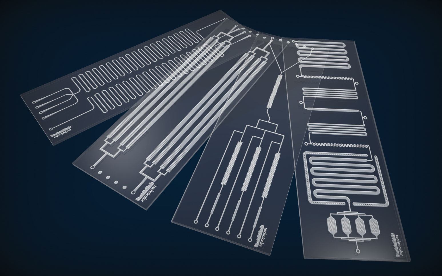
Manufacturers of digital media may play an important role in the scale-up of microfluidics and lab-on-a-chip design as well. Technicolor, most notable for its contribution to film coloring and in-home entertainment, is one of the most novel players entering the emerging market space for injection-molded microfluidics and lab-on-a-chip technology.
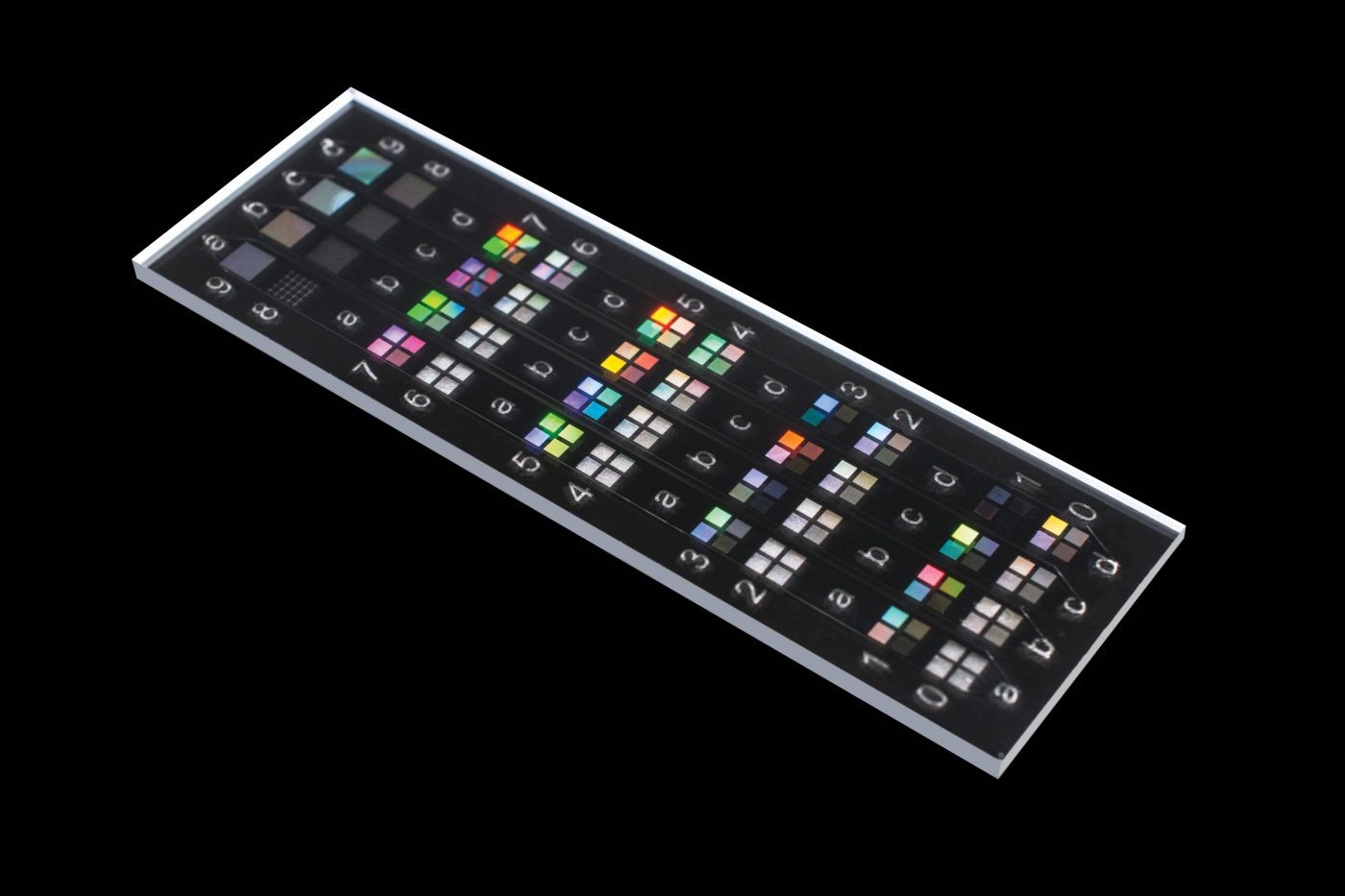
In 2018, Technicolor presented a prototype chip at the Lab-on-a-Chip World Congress that can amplify a fluorescence signal eightfold by integrating optical diffractive lens technology into the chip. To do so, the chip, a multilayer device, uses a proprietary process originally developed by Technicolor in the optical media industry. The chip’s performance captivates the scientific audience, which is interested in detecting very small variations in signal resulting from precise chemistries on chips. The chip also displays Technicolor’s abilities in micromilling, bonding, and fine-feature lenses.
John Town, senior vice president of technology at Technicolor, indicates that the company’s initial entry into the scientific market space was in 2016. At that time, Technicolor was still matching internal capabilities to market requirements. Specifically, the company was compiling a long list of manufacturing processes used in the production of optical media that could be applied to microfluidic device design. These processes include photolithography and laser lithography for etching surfaces and state-of-the art injection molding using polymers such as cyclic olefin copolymer (COC) and cyclo olefin polymer (COP).

Town says that Technicolor is uniquely positioned to capitalize on this market’s growth due to the company’s preexisting global manufacturing capacity, which includes cleanroom fabrication and assembly facilities, and options for packaging and supply chain management. “Manufacturing areas within each Technicolor facility are facilitized for injection molding, lithography, and electroforming,” Town asserts. “They are ideally prepared for lab-on-a-chip manufacturing expansion.”
The microfluidics/lab-on-a-chip industry differs from the optical media industry, Town says, with respect to standardization. In the optical media industry, specifications have been standardized the world over, but microfluidic devices and form factors will differ depending on the chemistry and science employed on the device, requiring smaller batches and additional assembly line retooling with each new device design.
Plastics for microfluidics manufacturing
Another manufacturer in the microinjection molding industry is Plastic Design Corporation (PDC). Located in Scottsdale, AZ, PDC is also a manufacturer of plastic microtiter well plates. PDC’s engineer, president, and founder, Mark Kinder, explains that the company’s microfluidics business “has grown faster than our microtiter plate business and represents approximately 60–65% of our labware business.” This market segment primarily serves the diagnostic industry. “Most of that,” Kinder points out, “is trying to match a DNA strand through the diagnostic.”
“What we are trying to do is miniaturize the whole lab process,” he continues. “The days of petri dishes and test tubes are gone. As we miniaturize it, the handling becomes more difficult, so why not incorporate it all on one platform, so that you don’t have to handle it after sample prep.”
Failed programs using novice microinjection molding companies have slowed the use of injection molding techniques in lab-on-a-chip design. “What happens is that the disposable—the cartridge—doesn’t get the attention early in the development process,” Kinder explains. “It is kind of a stepchild. It’s a plastic part.” According to Kinder, the customer thinks, “Anyone can make that.” So, the customer goes to a molder, who says, “Of course we can make that.” Unfortunately, the molder builds a cheap mold. The parts don’t work, or they work for small batches, leading to mounting errors during the scaling process. “If you are manufacturing 10 or 20 cartridges, the errors don’t show up,” he notes. “But if you are manufacturing 200 to 300 thousand a month, all of a sudden you have a 2–3% dropout rate.” These failures add considerable cost to the manufacturing process.
To combat these issues, Kinder encourages the building of strong relationships with your molder, as well as early discussions on design requirements for molded devices, such as the need for appropriate draft angles in channel walls that aid in removal from the mold. He and his team have also responded to the needs of customers by specializing in reducing manufacturing errors and using better materials.
“There are two materials of choice if you are going to do optical scans or fluorescent scans,” he points out. One is COP, a homopolymer; the other is COC. The COCs are more commonly used but can lead to increased leeching into your product, especially during lengthy storage. Leeching can affect the precise chemistry within the cartridge.
“We haven’t seen any evidence of leeching with COP,” Kinder notes. However, the manufacturing process for utilizing COPs is more complex than that for COCs. A key problem is that during manufacturing, COPs can absorb oxygen. To overcome this problem, PDC has adapted its facilities to perform resin drying in a nitrogen dryer, and to use nitrogen-blanketed injection and extrusion during the molding process.
Glass in microfluidics manufacturing
IMT Microtechnologies in Zurich is a foundry that works with clients to develop glass consumables for the diagnostic and life sciences markets. The company’s products are used in microfluidics and lab-on-a-chip flow-cell manufacturing. Like other manufacturers that serve the microfluidics/lab-on-a-chip market, the company applies expertise and competences it has gained by serving other markets. IMT Microtechnologies has experience in supplying the semiconductor industry, enabling medical and dental applications, and facilitating the integration of optical technology.
“We use the microfabrication expertise originally developed for microelectronics into flexible and scalable solutions for the manufacturing of micro- and nanostructures in glass for consumables in life sciences applications and components in medical instruments and equipment,” says Alexios Tzannis, PhD, business development manager, life sciences, IMT Microtechnologies. “We use lithography techniques, for example, to etch structures in glass to make the microfluidic channel network. We use classical fusing bonding to create what we call passive components.”
The company also specializes in creating active components. For example, some of these components incorporate electrodes for electrical impedance spectroscopy and dielectrophoresis applications, and others incorporate waveguides for fluorescent detection applications. The devices that contain waveguides, Tzannis explains, “have a very thin layer of dielectric where light propagates to excite fluorophores bound to the analyte that have been immobilized on the surface of the channel.” When devices contain waveguides, they can decouple the excitation wavelength from the emission fluorescence within the channel to perform high-throughput screening with reduced background signal. This functionality is extremely important when the fluorescence signal is low.
The company has refined techniques to apply immobilization chemistry on glass. These techniques can be used to make dots that bind analytes within the microfluidic channel. “When, say, FX proteins pass by, they will have an affinity to stick there,” Tzannis notes, “and we can do this at the micrometer scale, let’s say 20–30 µm, for protein analysis, or at submicrometer level for next-generation sequencing.”

Glass is considered to be an expensive material for microfluidics design, but according to Tzannis, it is a material that “has extremely good chemical, electrical, and physical properties.” It has a very high dielectric constant—useful for electrical measurements—and is better for studies performed at high pH and in high temperatures, such as studies involving PCR. Glass can also be useful in applications requiring lengthy analyses and multiple measurement detections. In next-generation sequencing (NGS), Alexios suggests that working with glass can facilitate high-accuracy manufacturing. Specifically, microfabrication expertise originally developed for microelectromechanical systems can be transferred into flexible and scalable solutions for the manufacture of micro- and nanostructures in glass. More than this, selected glass materials offer low autofluorescence, a critical attribute in devices that capture weak fluorescence signals to enable applications such as NGS and single-molecule assays.
When customers consider whether glass is a suitable platform, they should, Alexios advises, ask a few essential questions: “What is my application/assay? How does this transfer into a business case? What are the critical parameters that are detrimental for the assay? How many measurements can I make on one flow cell? How much revenue do I get back from the flow cell? In addition, customers should consider hybrid solutions that combine the advantages of different material platforms. Doing so might lead to affordable and successful commercial assays for the life sciences and diagnostics markets.”
New Microfluidic Screening Platform Introduced
Efficient Robotics recently introduced a microfluidic screening platform that enables the processing of microbial and mammalian cells, enzymes, proteins, antibodies and
peptides at an ultra-high-throughput of up to 10 million samples per day, according to Martin Mitchell, global marketing manager.
The Nano-Titer-Pipe (NTP) Screening Workstation allows the continuously fully automated processing of inoculation of droplets with single cells, timely defined incubation of each droplet with controlled O2 and CO2 exchange for defined generations of cell growth, assay addition of fluorescent-based and light-scattering assays, assay incubation, as well as detection and selection of hits, he notes, adding that the system is easy to handle and can be operated with no manual intervention needed.
“The platform has an outstanding precision over the whole processing of droplets of less than 2% CV by an active controlled pressure and valve system,” says Mitchell. “The platform’s other advantages include its defined incubation time, which can be exactly stopped during the exponential or stationary growth phase of cells; its high sensitivity of fluorescent detection at low picomolar range; and its flexibility and modularity to cover different screening setups.”
